top of page
 Sync Board IISystem test with LM134 current sources showed artifact in rising edge, prompting v1.3 to use Schmitt buffers instead |  Sync Board IIv1.3 |  Sync Board IIKiCAD 3D model of sync board under development. Note six outputs (left, front) with jumpers for options set by two 8-bit dip switch banks (right, front). |
|---|---|---|
 Signal ArtifactUse of LM134 current sources to power indicator LEDs from output signal caused a current draw after a turn-on delay of 6 microseconds. Resulting falling edge would be enough to trigger a falling-edge-detect, so a redesign was thus required. |  Signal ArtifactOn an output signal without the LED and LM134 current source, the trace rises as normal, strongly identifying the extra current draw as the issue. |  Sync Board IIKiCAD schematic showing circuit architecture. |
 Sync Board IIPCB Editor in KiCAD showing footprint layout. |  VivadoSim, First HarmonicSimulation of Verilog HDL program defining two synchronized signals at the 1st harmonic. |  SyncBoard_IPrevious synchronization board in KiCAD. Note JST-XH Connector pads around outside, and two SOIC-14 footprints where the SN74LS07DR level-shifters are placed. The drawback of this original board is it can only split out and amplify a single input signal. |
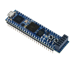 Cmod_A7-35T_Artix7_FPGAThe Digilent Cmod A7 35T FPGA with Artix-7 fabric will plug directly into a custom board. The carrier board will handle power and protections such as reverse polarity. |  RP2040_1Sketches of an early design concept using an RP2040 microprocessor. Incoming signal may be modified in an assembly level program with deterministic timing cycles. Outputs are available at 3.3V or 12V. |  RP2040_2Sketches of an early design concept using an RP2040 microprocessor. Incoming signal may be modified in an assembly level program with deterministic timing cycles. Outputs are available at 3.3V or 12V. |
 RP2040_3Sketches of an early design concept where DIP switches would toggle output levels between 3.3V and 12V. |
bottom of page